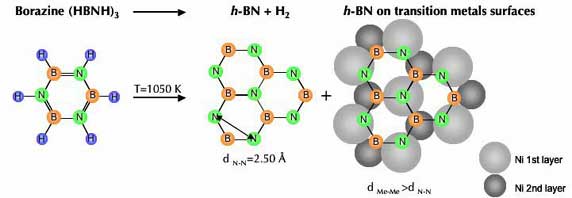
Different complementary experimental techniques are used to study the
boron nitride Nanomesh on
Rh (111):
Scanning tunneling microscopy (STM)
allows to take a direct look on the local real space structure of the surface, while
low energy electron diffraction (LEED)
(more details) patterns are formed
by surface structures ordered over a macroscopic sample area.
Ultraviolet photoelectron spectroscopy (UPS)
gives information about the electronic states in the outermost atomic layers of a sample, while
X-Ray Photoelectron Spectroscopy (XPS)
allows to get information about the electronic states of the innermost atomic layers.
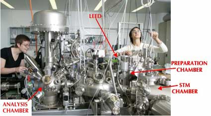
Zurich's experimental setup is shown, where it is possible to perform photoemission,
LEED and
STM measurements on the very same sample surface under
UHV.