Google search nanomesh.ch

Other forms of boron nitride on transition metals

Monolayers of hexagonal boron nitride on transition metals form a class of interface systems with properties of a metal-insulator interface. They are thermally stable, chemically inert and form well defined tunneling barriers.

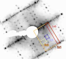
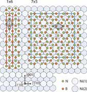
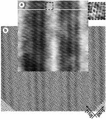
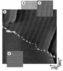
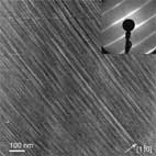
In the past h-BN layer(s) have been studied on Pt(111), Ru(0001), Cu(111), Ni(111) and Ni(100). The nanomesh could till now only be observed on Rh(111) and Ru(0001). Here we present our results of h-BN evaporated on Ni(110), Pd(111), Pd(110) and Mo (110), where no nanomesh but other forms of boron nitride are observed, which are all forming a monolayer on the substrate .

h-BN on Ni(110)

LEED pattern (left) and atomic model (right) of h-BN on Ni(110).
The size of the unit cell of hexagonal boron nitride is very similar to the one of the Ni(110). The lattice mismatch is only of 0.5%. LEED patterns show several h-BN superstructures, namely (1x6) and (7x5), which are schematically shown in the figure on the left. No consistent overlayer model has been found for the (6x3) structure. It is believed that the (1x6) structure is more abundant than the (7x5) one.


h-BN on Pd(111)
Like on Ni(110), boron nitride layers are formed on Pd(111) with two preferred structures. A (10x10) superstructure along the Pd crystallographic directions and an incommensurate structure rotated by 30o are mostly present on the surface. Further Moiré patterns are also present with different azimuthal rotation angles between the substrate and the boron nitride layer. A Mo iré pattern is observed when two layers with different periodicities are superimposed. The model of the rotated structure is shown on the right, where black and dark grey circles represent the B or N atoms, respectively, while the light grey circles stand for the Pd atoms.

These results show that the lattice mismatch is not the only key ingredient for explaining the different BN structures since Rh(111) and Pd(111) have comparable ones (-7% and -9%), but no nanomesh is observed on Pd(111).

STM image (left) of h-BN on Pd(111). A Mo iré pattern is visible. The size of the image is 20 nm x 20 nm. On the right a model of rotated h-BN.


h-BN on Pd(110)

STM images of h-BN on Pd(110), which forms several Mo iré patterns. The left image (a) has a size of 10 nm x 10 nm, and the right one (a) 50 nm x 50 nm.
Like on Pd(111), the h-BN units do not find a unique way to register with the Pd(110) surface. Indeed, they form a large variety of domains with respect to the substrate crystallographic directions while preserving their original inter-atomic distances. Some Mo iré patterns resulting from the superposition of substrate and film periodicities are visible in the STM images on the left. Simulation of such Mo iré pattern are visible beside the concerned STM measurements (see b on the left and b-c-d images on the right). No predominant Mo iré pattern could be identified.


h-BN on Mo (110)

Two distinctly different self-assembling nanostructures form on Mo (110) after exposure of the surface to borazine. Both structures show one-dimensional characteristics, but in directions perpendicular to each other.

When the deposition of borazine is carried out at preparation temperatures of about 950K, a graphene-like h-BN structure forms, as can be seen in the left image. It consists of a single boron nitride layer, which forms stripes spaced of 1.26 nm each other.

When the borazine exposure is performed at higher temperatures like 1170K, a very different phase appear, namely B nanowires, as can be seen in the right image. At such temperature all nitrogen has disappeared during preparation. The wires are 2-10 nm wide and up to 1 μm long. This leads to extremely high aspect ratios of up to 500.

It is possible to grow the two phases in coexistence when the preparation temperature ranges in-between 950-1170k, what renders this system extremely interesting as a template to align molecules or nanotubes very precisely.
       
STM images. On the left a graphene-like h-BN layer forms at low temperature (950K). At higher preparation temperature like 1170k, B nanowires appear, like on the right image. LEED pattern in inset.


Webmaster
| Last update: 25.03.2008 by C. Galli Marxer