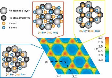
All these information allowed to simulate the full nanomesh, which is presented
on the right. The upper right figure shows a map of the high of the
N atoms with respect to the
Rh surface.
The blue "circles" correspond to the pores, where the nanomesh lies at the nearest of the
Rh surface
at a distance of about 2.2
Å. The wires around the pores have two different regions.
The red one is 2.7
Å above the surface, and the yellow one sits 2.5
Å above the Rh.
An atomic distribution model of these three main regions is also given.
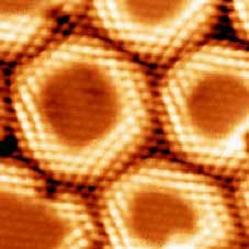
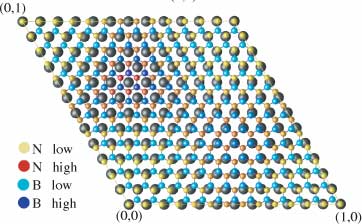
This model reproduces perfectly STM measurements of the nanomesh (image just above this text)
taken at 77K. In STM measurements of the nanomesh, only
N atoms are visible. The comparison with
the map on the right is therefore possible.
At such cold temperatures the atomic movements are reduced, allowing to
get images with very high resolution. Each "ball" corresponds to an
N atom. This image shows
that the nanomesh forms a continuous layer with visible pores.
The lower right figure shows the arrangement of the
B,
N and
Rh atoms over one
unit cell (delimited by black lines in the upper map).
This model shows clearly that
N (yellow) sits exactly on top of
a
Rh atom only in the middle of a pore, while
B (light blue) sits exactly in-between
Rh atoms.
The position of the
boron nitride atoms relative to the
Rh ones is always more shifted when you
go from a pore to a wire. At the highest region of the wire,
neither
N (red) nor
B (dark blue) sit on top of a
Rh atom, but they form an hexagonal ring around it.
In the lower part of the wires, colored in yellow in the
map, the
B sit on top of the
Rh atom.