In 2003 M. Corso
et al. from
Osterwalder's group at the
University of Zurich, Switzerland, published in
Science
[M. Corso et al., Science 303, 217 (2004)]
the discovery of a new inorganic nanostructured two dimensional material, called nanomesh, which so far
has no analog in
systems composed of carbon.
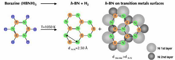
The discovered
boron nitride nanomesh is composed of
boron (B) and
nitrogen (N)
atoms, which form
a highly regular mesh after
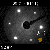
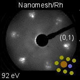
high-temperature exposure of the clean
rhodium
(Rh (111))
single crystal to
borazine
.
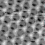
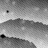
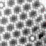
The nanomesh has a
honeycomb-like superstructure (see figure) with apertures of 2
nm
and wires of 1
nm.
In 2003 a double-layer model was proposed, where each
BN layer
was offset in such a way as to expose a minimum metal surface area.
In
2007 an alternative model emerged, which consists of a full single
BN
layer (no more holes), where "pores" are
closer to the crystal surface than the wires.
The formation of the nanomesh is a
self-assembly process,
i.e. the organisation of the atoms is driven by the nature itself without any human intervention.
The
self-assembly process is likely driven due to close but
different periodicities (
lattice constants)
of the
BN nanomesh and the
Rh substrate and a site dependent BN-bonding to the substrate.
The
boron nitride nanomesh is stable towards air, vacuum and liquids, and it does not
decompose up to temperatures of at least 796C (1070 K).
In addition the
BN nanomesh can serve as a template to organize molecules, as is exemplified by the
decoration of the mesh with
C60 molecules.
These characteristics promise interesting applications of the nanomesh in areas like
nanocatalysis,
surface functionalisation,
spintronics,
quantum computing
and
data storage media
like
hard drives.